
- Products
-
Optical Components
-
Optical Crystals
-
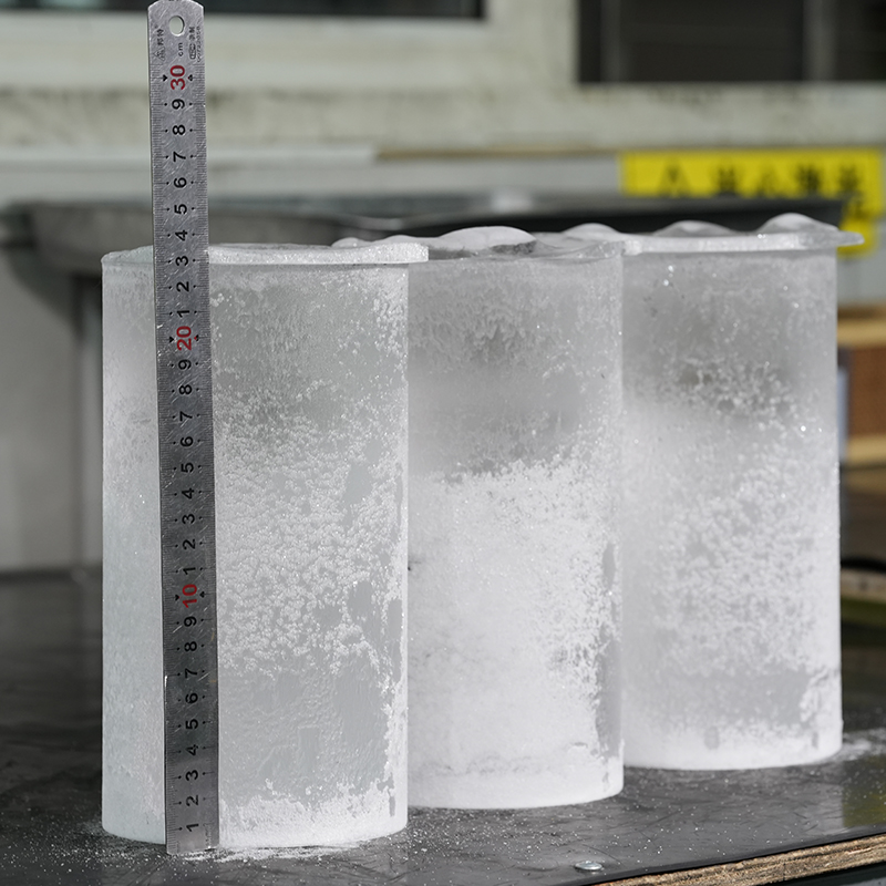
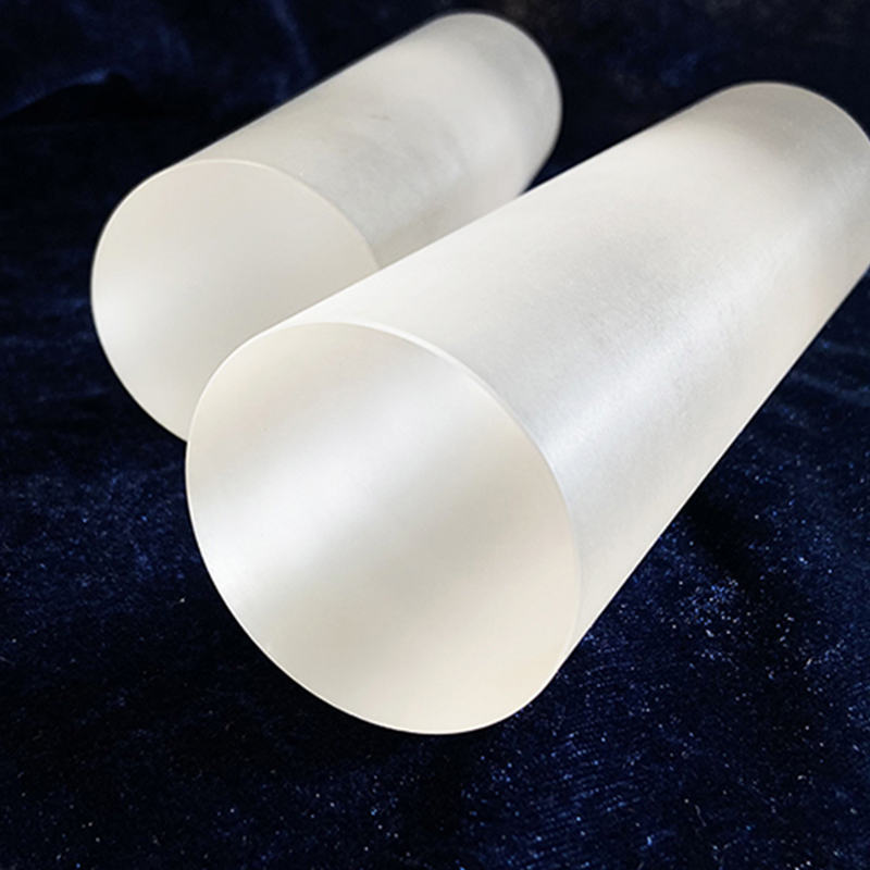
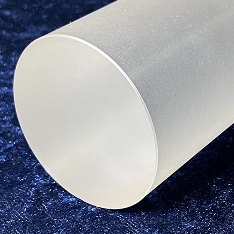
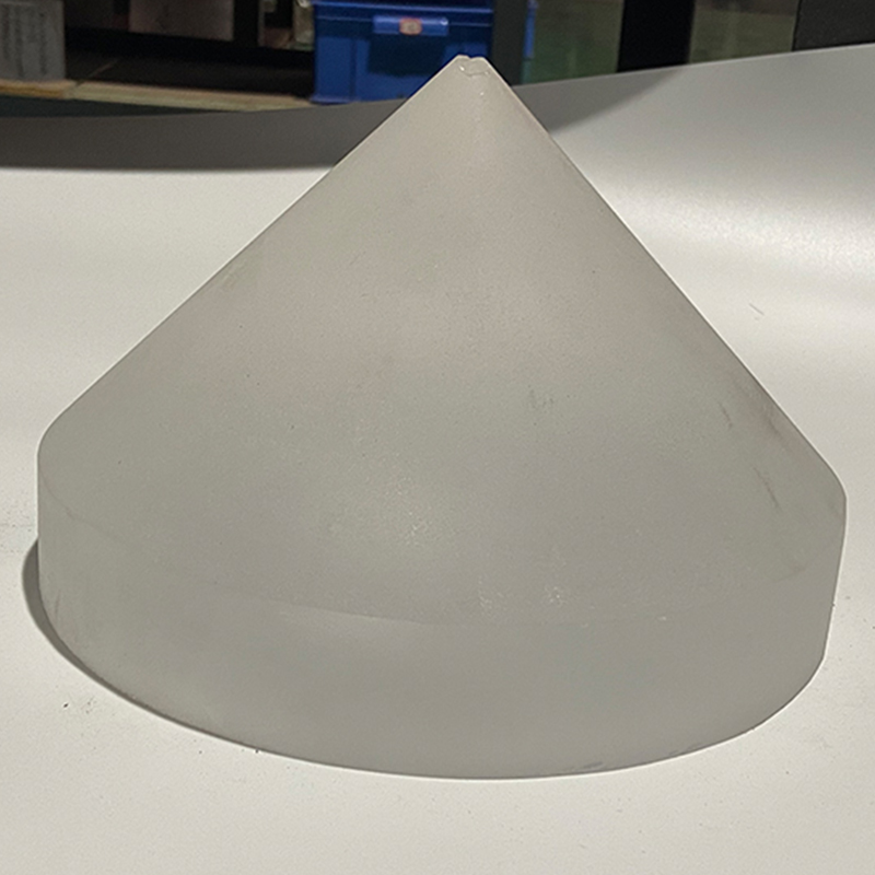
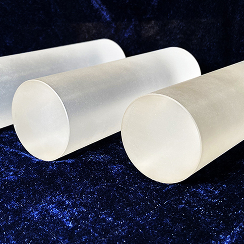
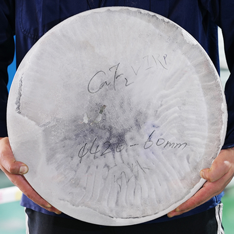
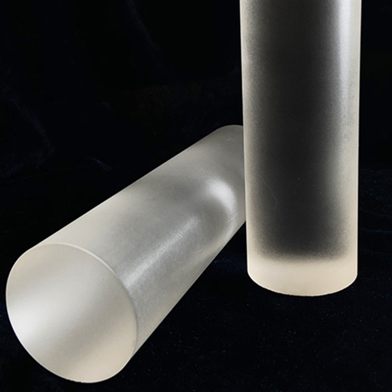
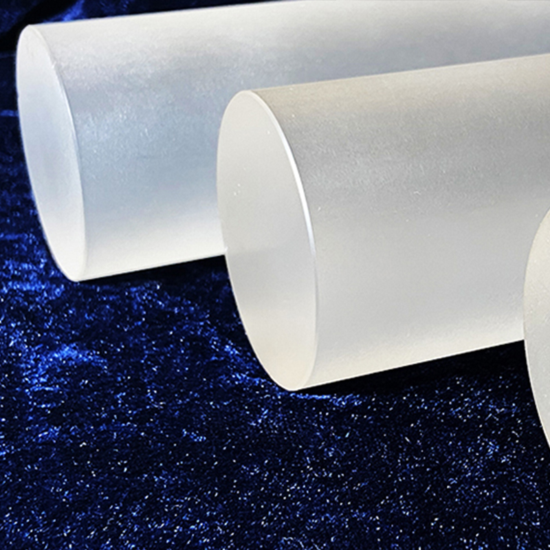
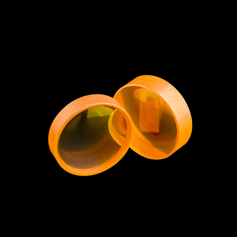
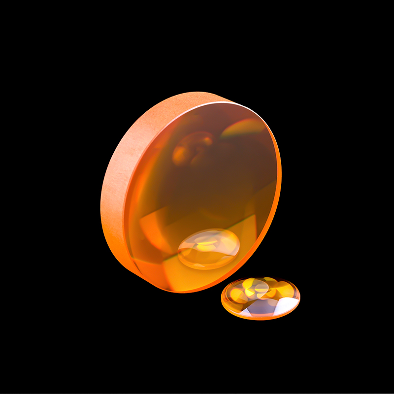
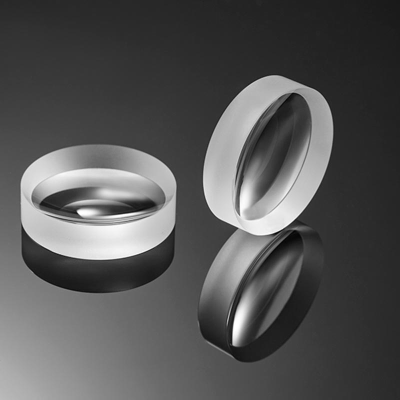
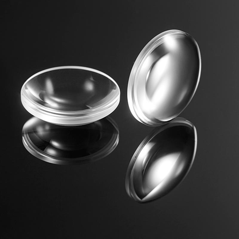
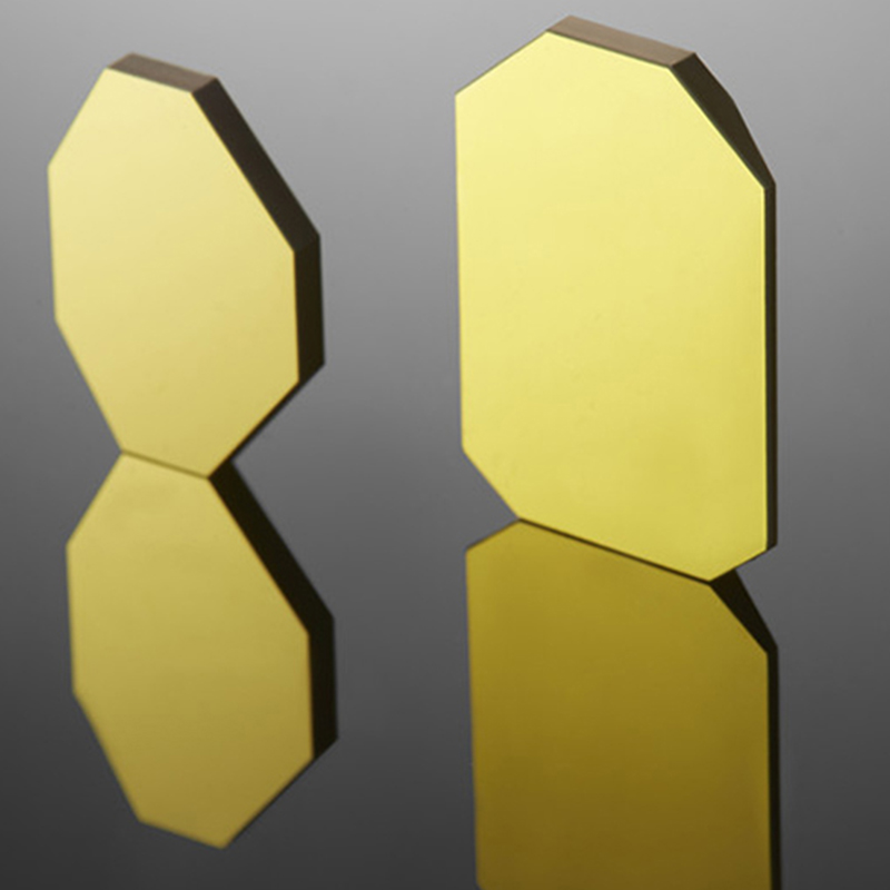
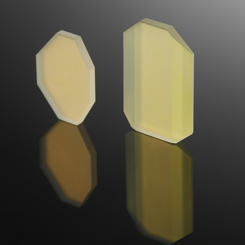
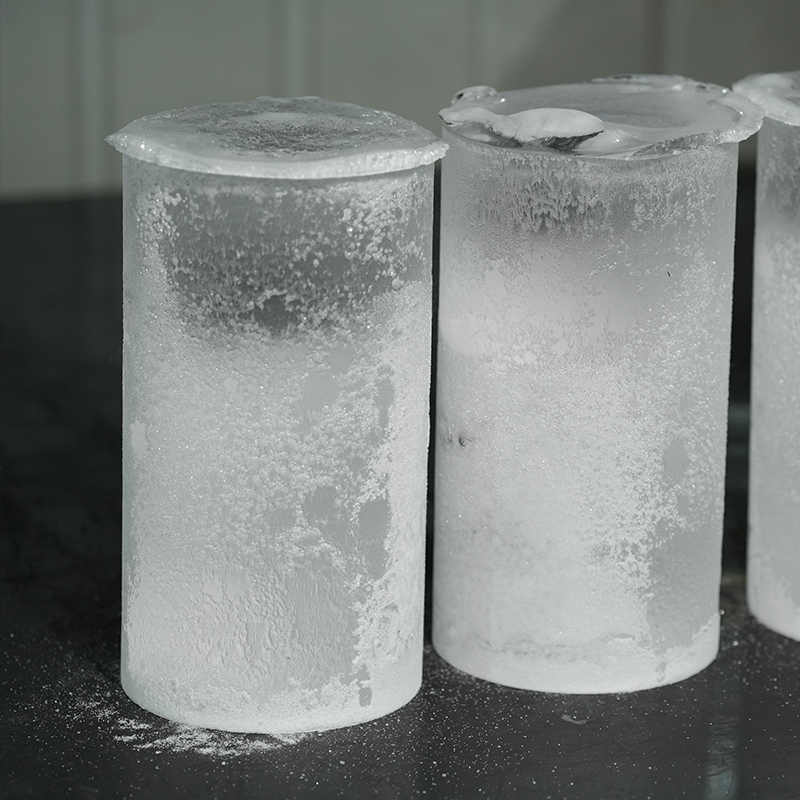
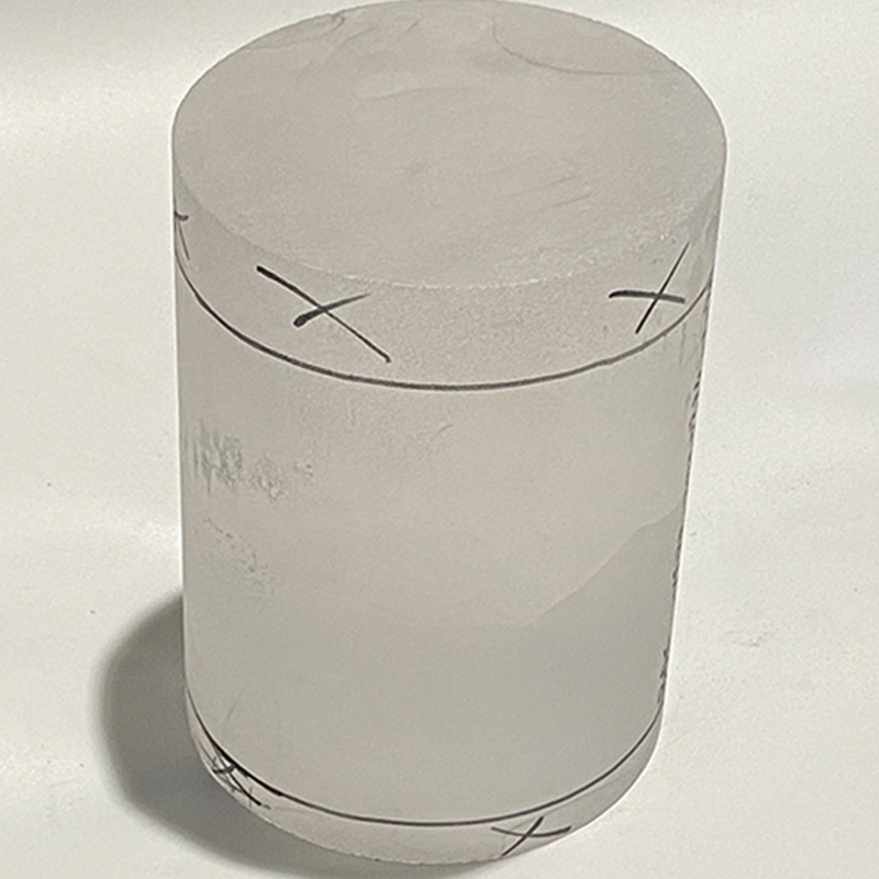
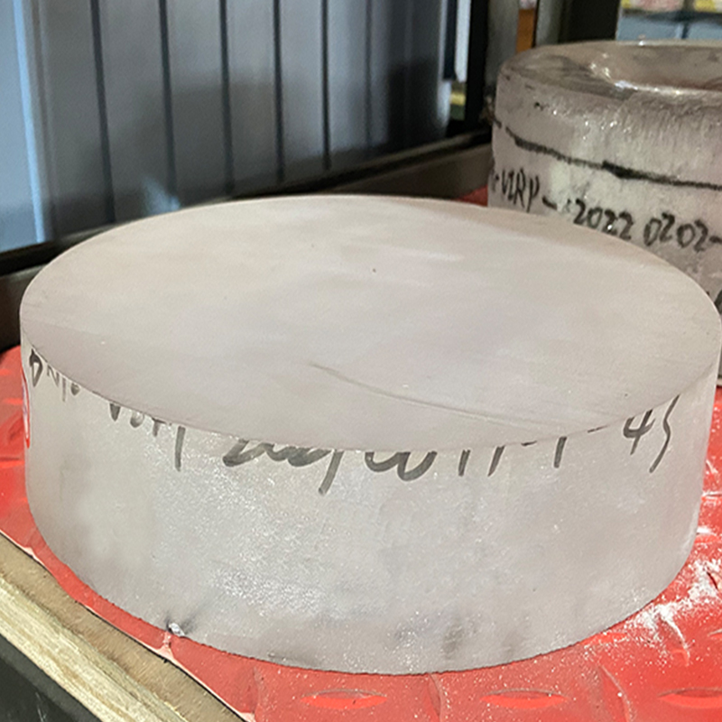
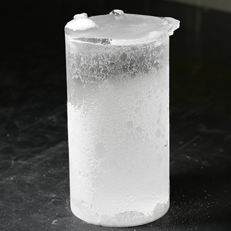
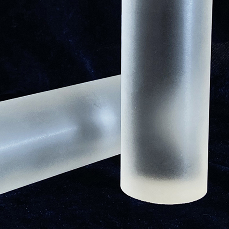
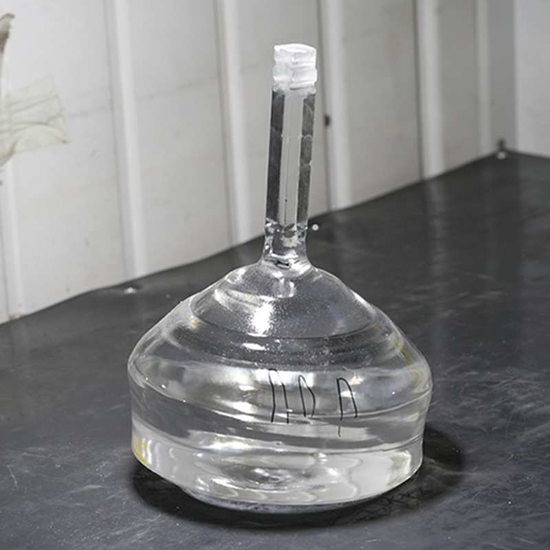
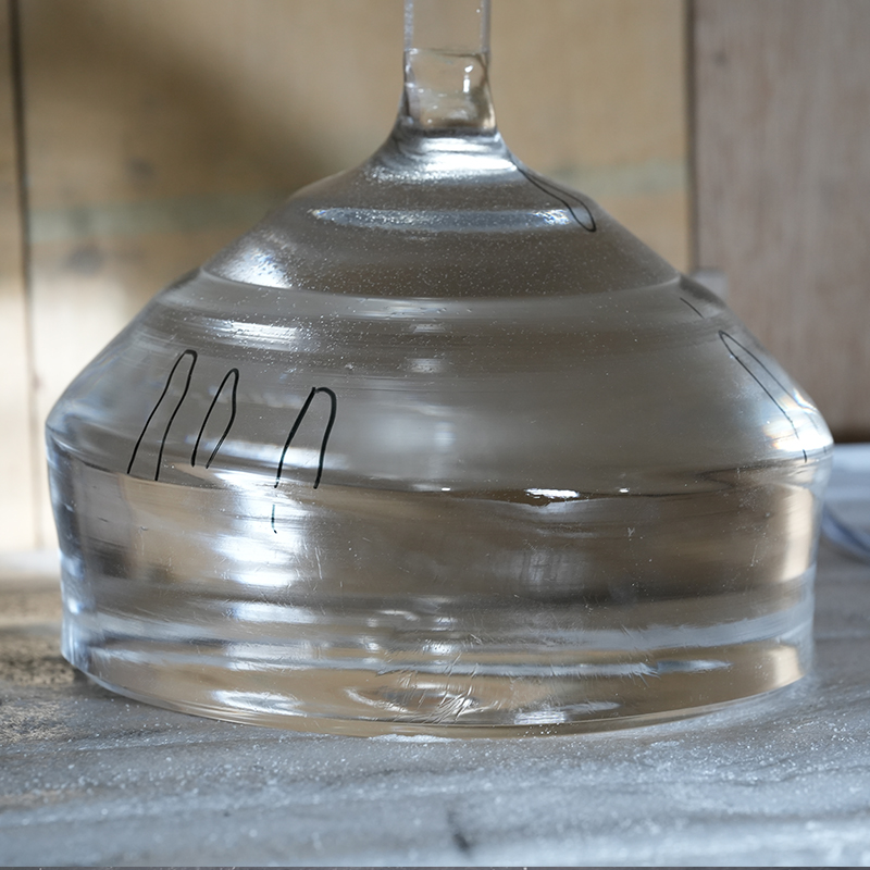
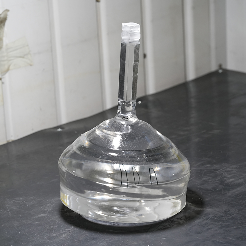
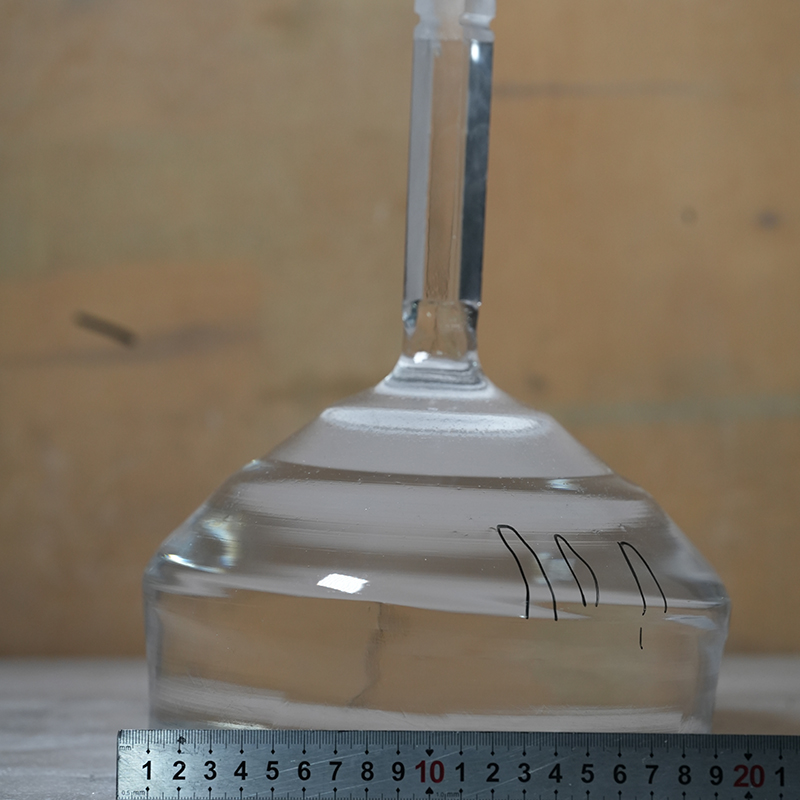
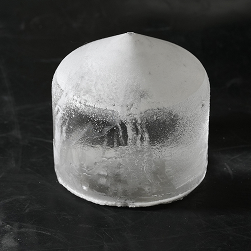
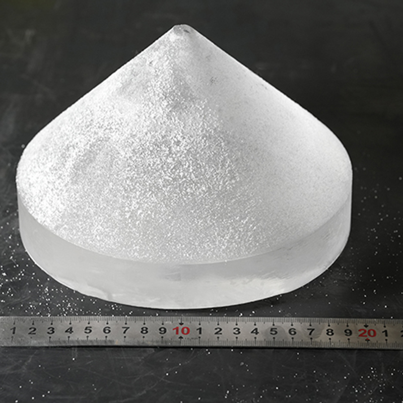
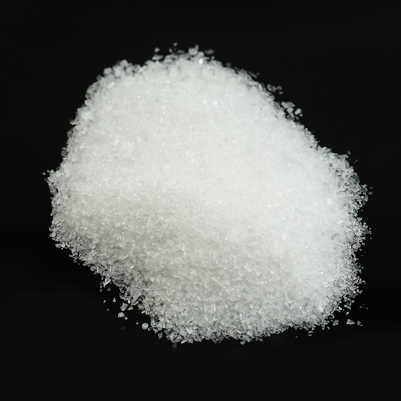
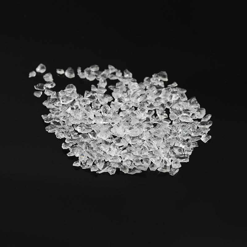
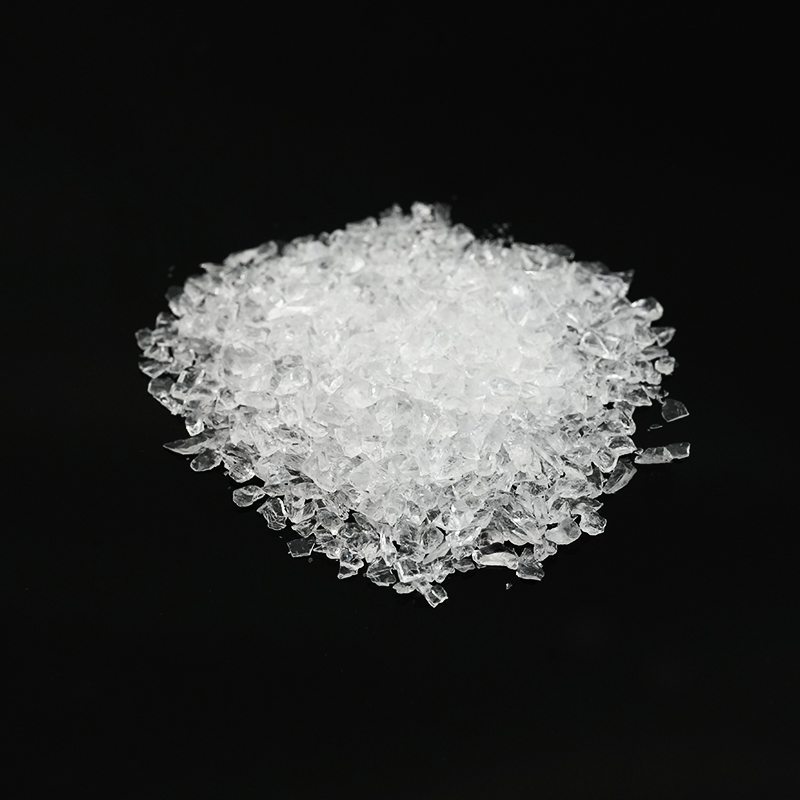
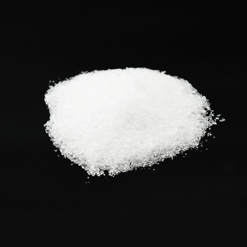
Calcium fluoride(CaF2)
-
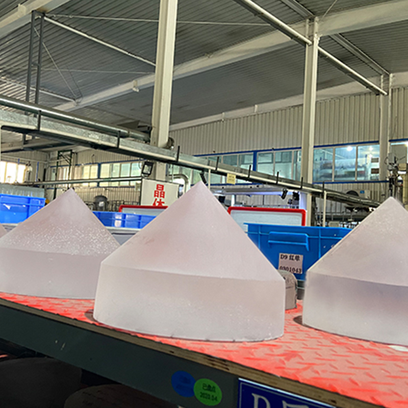
Single crystals calcium fluoride
-
Polycrystalline calcium fluoride
-
Infrared calcium fluoride
-
Ultraviolet calcium fluoride
-
VUV grade calcium fluoride crystals
-
Oriented calcium fluoride
-
Low stress calcium fluoride
-
Large size calcium fluoride crystals
-
Excimer grade calcium fluoride crystals
-
Non-fluorescent/ raman grade calcium fluoride
-
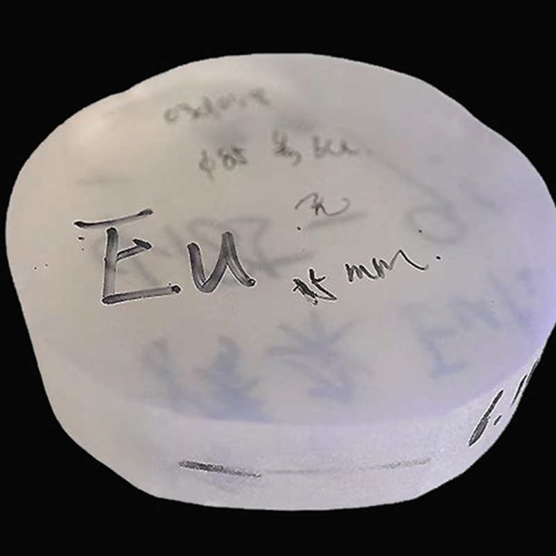
Eu:CaF2 scintillation crystal
-
- Barium fluoride
- Magnesium fluoride
- Lithium fluoride
- Silicon
- Germanium
- Zinc Sulfide
- Zinc selenide
-
Calcium fluoride(CaF2)
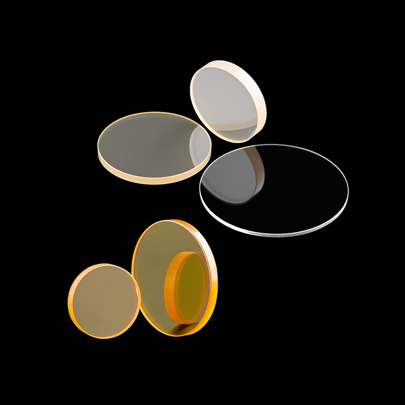
- Optical Coating
- Coating Materials
-
Optical Components
- About Us

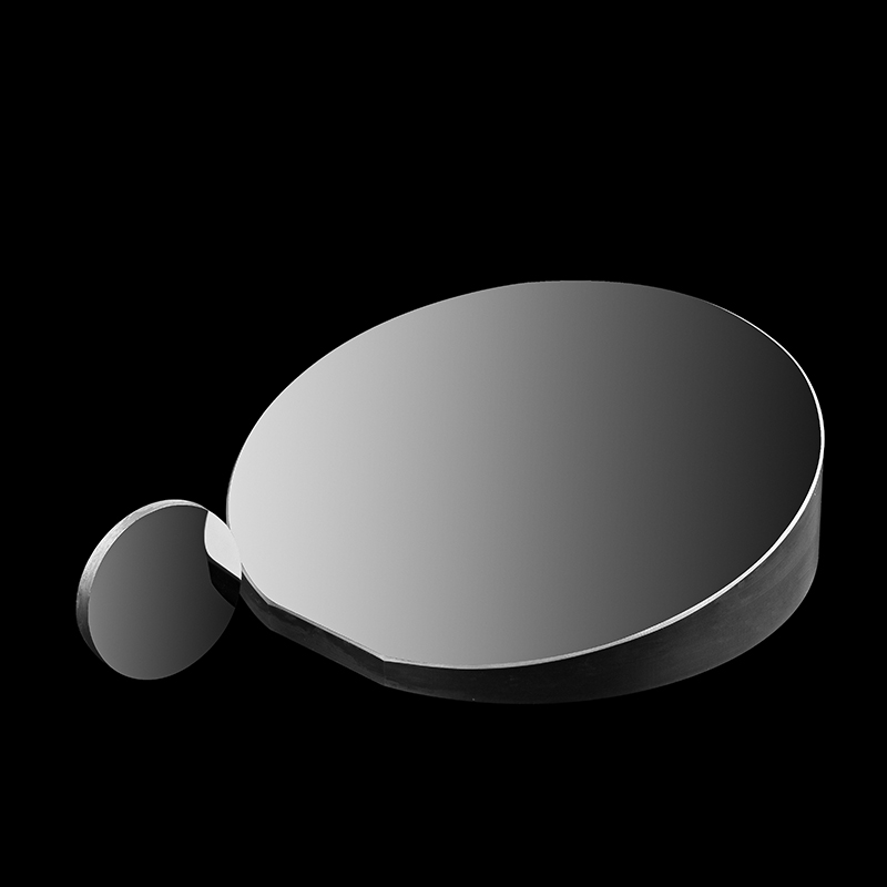


Silicon wafers
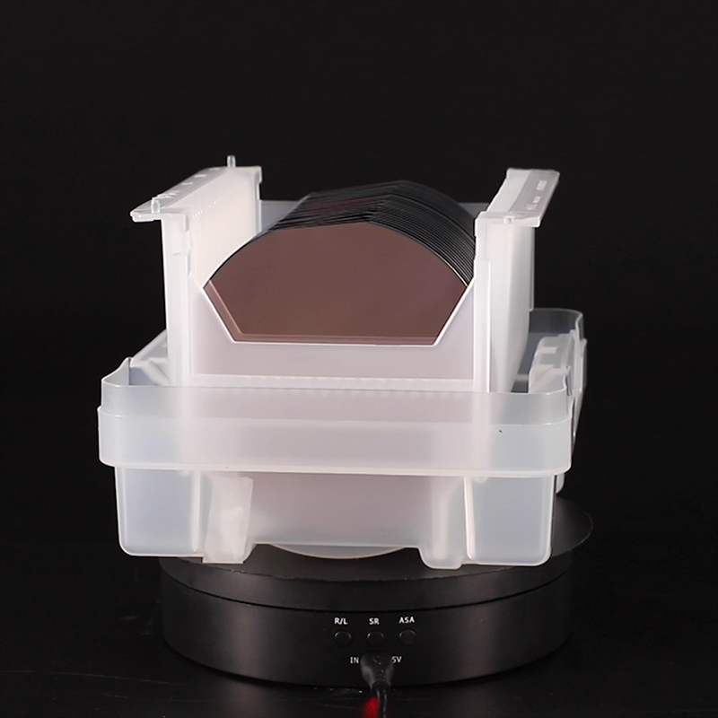


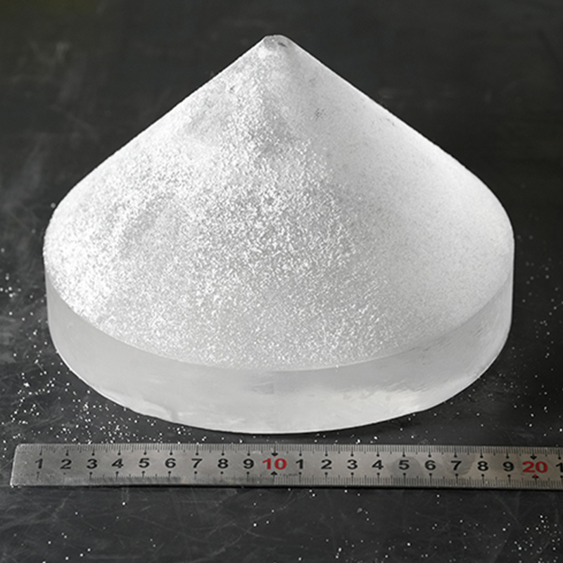
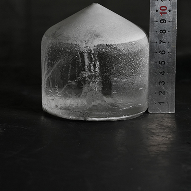
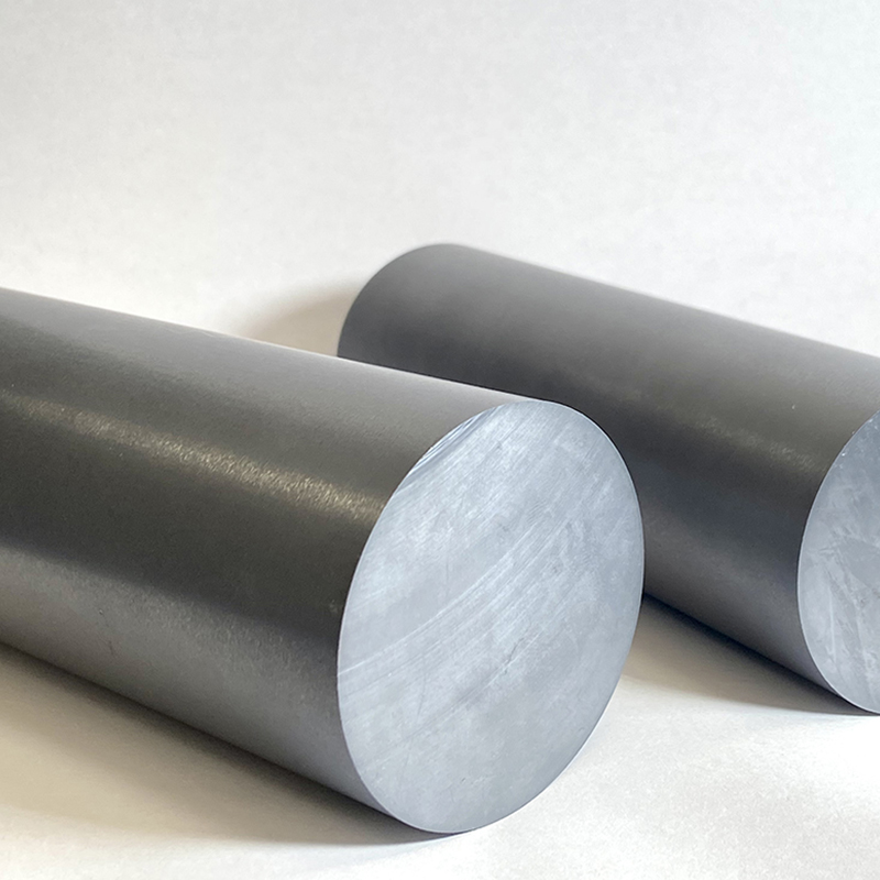
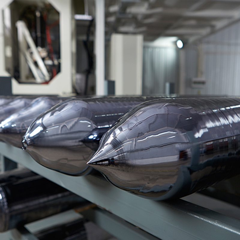
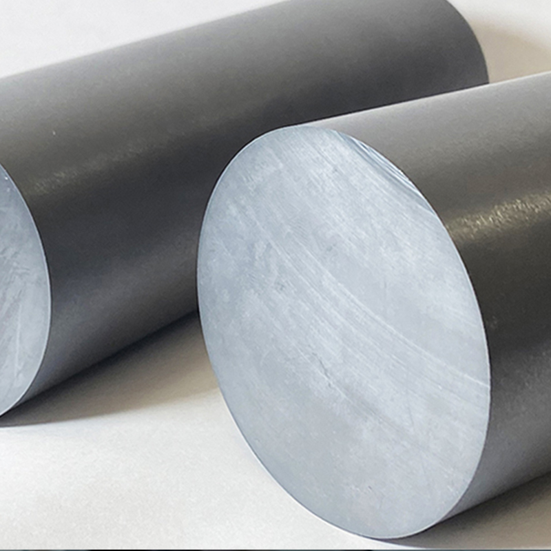
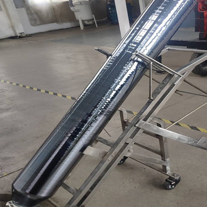
Single crystal silicon is commonly used as a substrate for 3-5μm mid-wave infrared optical windows and optical filters due to its good thermal conductivity and low density. It is also a commonly used material for making laser reflectors, infrared thermometry, and infrared optical lenses. Our company covers various process steps for silicon wafer processing, including material growth, cutting, polishing, coating, and dicing, with strict control over quality, delivery time, and price, and can provide both customized and batch production.We can provide 2-inch, 4-inch, 6-inch and 8-inch silicon wafers of CZ,FZ and intrinsic silicon.

Single crystal silicon is commonly used as a substrate for 3-5μm mid-wave infrared optical windows and optical filters due to its good thermal conductivity and low density. It is also a commonly used material for making laser reflectors, infrared thermometry, and infrared optical lenses. Our company covers various process steps for silicon wafer processing, including material growth, cutting, polishing, coating, and dicing, with strict control over quality, delivery time, and price, and can provide both customized and batch production.
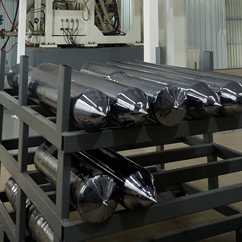
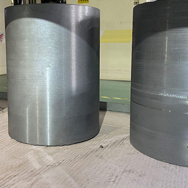
Silicon wafer processing requires highly skilled technicians and advanced equipment to ensure that the processed wafers have high surface smoothness and dimensional accuracy, while also ensuring that processing costs and lead times are controllable. Our company has an independent production line for silicon wafer processing, covering the entire industry chain from material growth, cutting, polishing, coating, to dicing. We are capable of producing silicon wafers of CZ,FZ and intrinsic silicon in various sizes, and can provide both customized and batch production to meet different customer needs.


Contact us
ServiceEmail:sales@umoptics.com
Phone:+86 17733572335
Whatsapp:+86 17733572335
Address:No. 100, Light Industrial Park, Shangcheng County,Henan


